


Product Center
产品中心

Product Features
Imaging mode: equipped with contact scanning, tapping scanning, electrostatic force scanning, magnetic force scanning, force curve, Kelvin function
Closed-loop resolution: XY axis: 0.2 nm, Z axis: 0.05 nm
Scanning range: XY axis: 40 μm × 40 μm, Z axis: 8 μm (upgradeable to 100 μm optional)
Conductive samples, insulating samples, biological samples Surface morphology and physical and chemical properties detection
(maximum sample size: 2.5 cm x 1 cm)
(Sample moving range: 12 cm x 12 cm)
Technical Parameters
Application Areas
Semiconductor wafer defect detection; material surface morphology, roughness, mechanical properties, local electrical properties, etc.; life sciences; biomedicine.
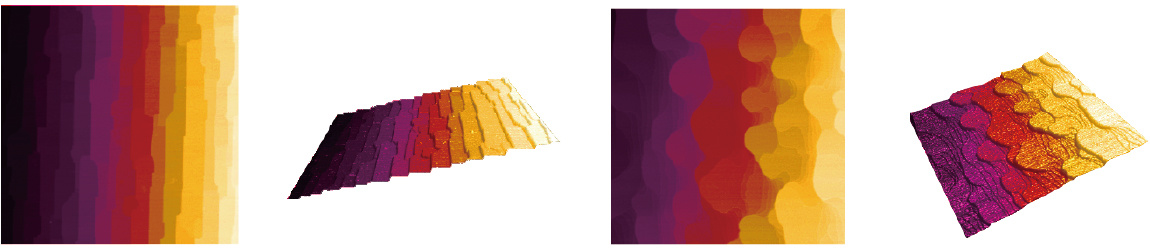
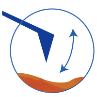
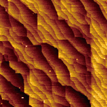
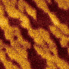
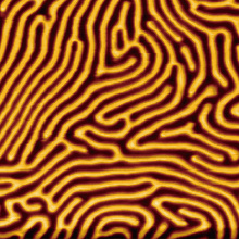
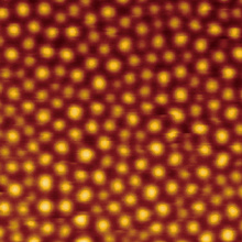
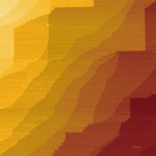
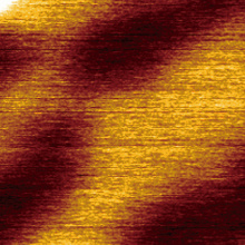
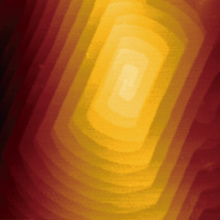
Product Imaging
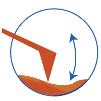
Tap Mode
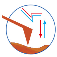
Contact Mode
Force curve
 |
 |
 |
 |
 |
 |
 |
| Surface charge distribution | Magnetic domain | Magnetic Bubble | Surface potential | Helical structure | ||
Keyword: Atomic Force Microscope AFM-NanoTech10
")


Online Message
If you have more needs, please leave a message. We will reply to you as soon as we receive the information!